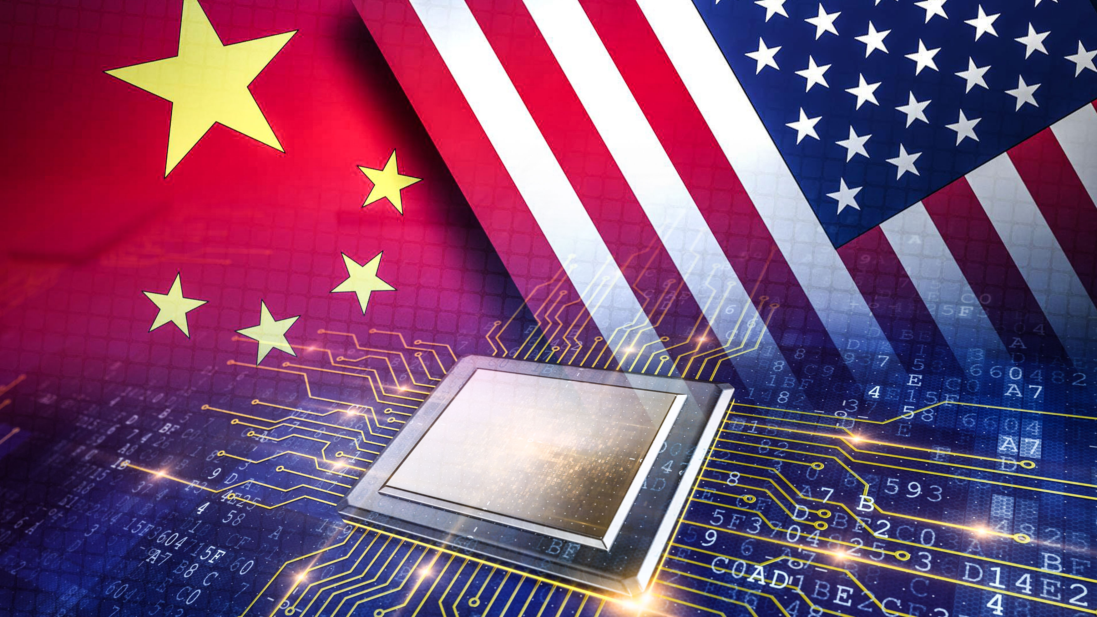
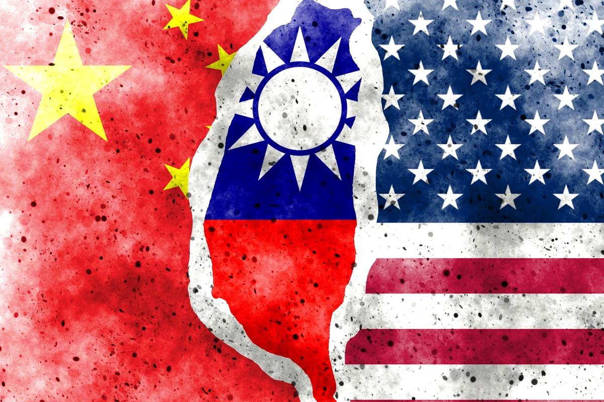
As U.S.-China tech rivalry enters a white-hot phase, export controls and talent restrictions imposed by the Trump and Biden administrations have not crippled China’s semiconductor industry. Instead, they have acted as a powerful catalyst, compelling the mainland to accelerate the construction of a “100% localized” supply chain. This progress has far outpaced external expectations, with prototypes emerging across lithography, foundry, and materials segments. Meanwhile, Taiwan’s long-relied-upon “Silicon Shield” narrative is under dual assault—from U.S.-driven “capacity hollowing” and China’s autonomous rise—leaving the island’s supply chain dominance increasingly precarious.
“Forced Innovation” Under U.S. Sanctions
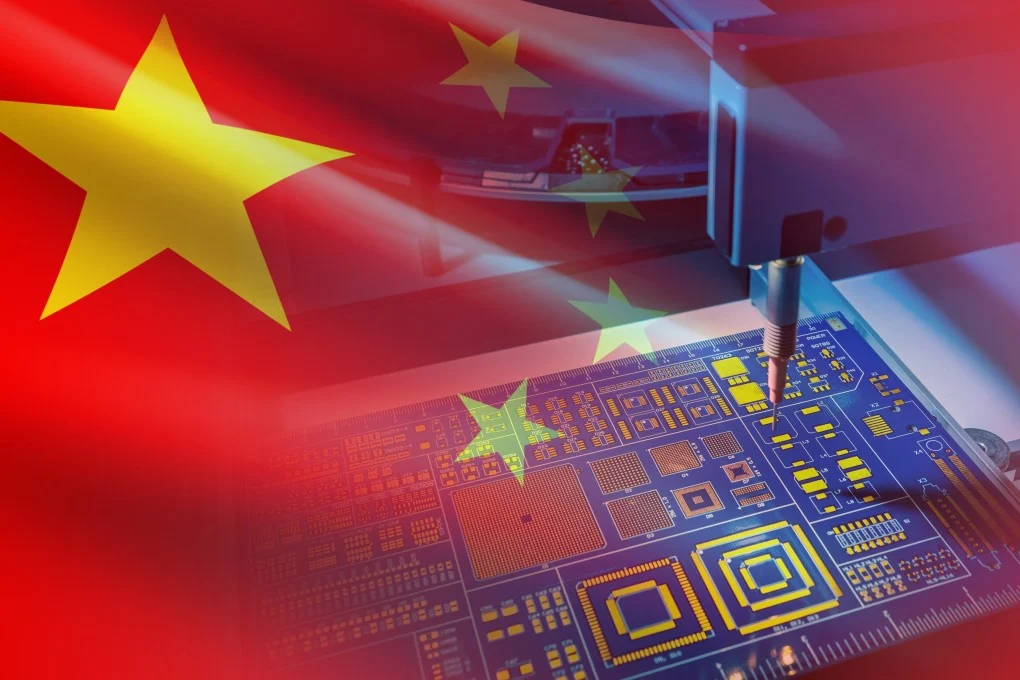
Since 2018, the U.S. Department of Commerce has placed Huawei, SMIC, and others on the Entity List, banning exports of sub-14nm process equipment and EDA software. The October 2022 “New Rule” extended controls to EUV lithography systems, GaN materials, and advanced AI chip design tools. On the surface, this is “choke-point” warfare; in reality, it has turbocharged China’s “whole-nation system” mobilization.
Huawei founder Ren Zhengfei set the tone in a 2019 internal speech: “Anything we cannot buy abroad, we will build ourselves.” Since then, HiSilicon has spearheaded a “one-against-seven” full-stack ecosystem, rallying hundreds of upstream and downstream partners:
| Segment | Key Player | Milestone |
|---|---|---|
| EUV Lithography | Xinkailai (Shanghai) | 13.5 nm core optical system breakthrough; prototype completed, entered pilot line in 2024 |
| DUV Lithography | Yuliangsheng (Harbin) | 193 nm immersion DUV scanner passed engineering verification; limited-volume delivery slated for Q2 2025 |
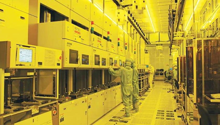
| Foundry | SMIC | Using domestic DUV + multi-patterning (quadruple exposure), pushed 28 nm tool resolution to 7 nm; FinFET yield reached 92% in 2024 |
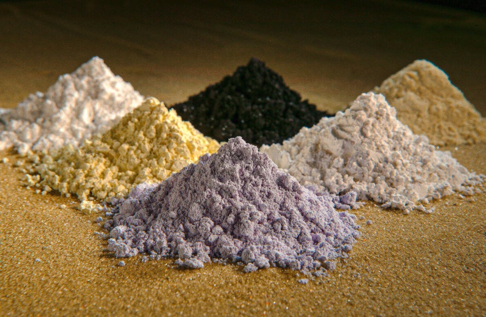
| Photoresist / Targets | Huali Industries, JF Electronics | ArF photoresist localization rate >60%; high-purity sputtering targets at 99.999% |
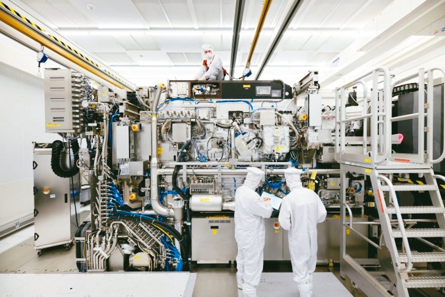
The DUV lithography machine stands out. In December 2023, Yuliangsheng completed the first domestic 193 nm immersion DUV “light-up” test at the Shanghai Microelectronics base, achieving 38 nm resolution (single exposure). Combined with SMIC’s quadruple patterning process, equivalent nodes below 7 nm are now feasible—meaning China can sustain mid-to-high-end chip volume production even without EUV.
Huawei rotating chairman Xu Zhijun stated bluntly at the 2024 Davos Forum: “Without EUV, 5 nm will be our ceiling for the next 3–5 years.” This is not capitulation but pragmatic planning—the Kirin 9000S (7 nm) has validated the path, and the next generation will leverage Chiplet + domestic DUV to deliver “3 nm-class” performance.
The “Silicon Shield” Mirage: From Umbrella to Hot Potato
The “Silicon Shield” was once portrayed as Taiwan’s “nuclear deterrent”—TSMC controls 55% of global foundry capacity and 92% of advanced nodes. Who would dare touch Taiwan? Yet this narrative is crumbling.
U.S. Think Tank’s “Scorched-Earth” Doctrine
A 2021 U.S. Army War College paper, “In a Taiwan Conflict, TSMC Fabs Should Be Destroyed,” sparked global outrage. The authors argued that selective demolition during evacuation would prevent advanced nodes from falling into adversary hands. Extreme as it sounds, it reveals Washington’s true priority: supply chain security trumps Taiwan’s security.
The “Twin-City” Capacity Shift
The Biden administration’s CHIPS and Science Act offers $52.7 billion in subsidies, with a key condition: TSMC must relocate over 50% of its advanced capacity to the U.S. As of 2025:
-
Phoenix, Arizona: 4 nm in volume production; 3 nm slated for 2026;
-
Kumamoto, Japan (TSMC-Sony JV): 22 nm automotive-grade, ramping by end-2024;
-
Taiwan Hsinchu/Tainan: Retains sub-2 nm R&D; volume production shifting offshore.
TSMC founder Morris Chang warned: “U.S. fab costs are 4–5× Taiwan’s, electricity 3× higher, and water scarce.” Yet under U.S. pressure, advanced-node hollowing on the island is irreversible.
Taiwan’s Vice
-
From the U.S.: Talent drain (over 3,000 TSMC engineers relocated to the U.S. in 2024); core IP must be shared with American partners;
-
From China: SMIC’s 7 nm yield nearing 90%; Huawei Mate 70 series expected to ship fully domestic SoCs;
-
Forced Choice: As U.S.-China confrontation intensifies, clinging to Washington risks losing the mainland market (still >40% of Taiwan’s exports in 2024); tilting toward Beijing invites U.S. sanctions.
Outlook: A Bumpy but Inexorable Path to Localization
China will not leapfrog TSMC overnight, but trend-wise substitution is inevitable. SEMI forecasts:
| Year | China’s Self-Sufficiency (14 nm & below) |
|---|---|
| 2023 | 16% |
| 2025 | 35% |
| 2030 | 70% |
The core bottleneck remains EUV lithography. ASML monopolizes the market with ~60 units annually, all under U.S. export controls. Xinkailai has cracked the light source and optics, but High-NA lenses still rely on Zeiss (Germany). Optimistic timeline for domestic EUV volume production: 2028–2030.
Yet as Ren Zhengfei puts it: “Parallel advancement, overtaking on curves.” China can bypass EUV via:
-
Chiplet heterogeneous integration;
-
Wide-bandgap materials (SiC, GaN) in new domains;
-
Quantum/photonic computing for generational leaps.
Conclusion: Relative Power in Realist Lens
Semiconductors are a “winner-take-most” industry, but not zero-sum. As China rises, the U.S. revives domestic fabs via the CHIPS Act, Samsung expands in Texas, Japan’s Rapidus targets 2 nm, and Europe’s Infineon dominates automotive.
For Taiwan, the “Silicon Shield” was never a shield—it was a mirror reflecting geopolitical brutality. Once the mainland achieves stable 7 nm volume and DUV supply, TSMC’s bargaining power will erode sharply.
Over the next decade, the global semiconductor map will shift from “Taiwan-centric” to “U.S.-China dual-core + multi-node bloom.” For China, the road is rugged but the direction clear; for Taiwan, only technological neutrality and market diversification offer a foothold in the storm.