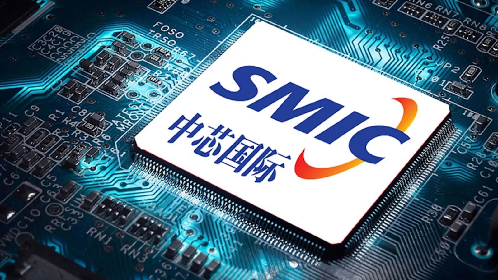
In the “arms race” of the semiconductor field, the lithography machine is undoubtedly the jewel in the crown. As the core equipment for chip manufacturing, it determines success or failure from design to mass production. Recently, prototype deep ultraviolet (DUV) lithography machines from Shanghai-based Yuliangsheng (UEA) have been reported as delivered to multiple wafer fabs, marking another milestone in China’s push for autonomy in high-end equipment. As early as September 2025, China’s largest wafer foundry, Semiconductor Manufacturing International Corporation (SMIC), began testing the country’s first domestic immersion DUV tool—not just a technical validation, but a critical step toward “self-reliance” in the global supply chain. This article delves into the “tuning” process: why it takes time, what exactly is being adjusted, and how much “time window” China has left amid the U.S.-China tech rivalry.
Multi-Track Parallel Development: More Than One Machine, More Than One Path
UEA’s DUV prototypes are not a lone effort. According to reliable reports, its subsidiary has shipped over 500 stepper lithography machines by August 2025, capturing 90% of the domestic market. These machines are not mere copies of Western technology but explore multiple technical paths to surpass existing performance. Industry sources suggest UEA may have delivered three prototypes to different wafer fabs for parallel testing—a plausible strategy, as China’s semiconductor development emphasizes “innovation over reverse engineering.” Simply “copying homework” would doom products to perpetual lag.
China’s path in semiconductor development has not been straightforward. As early as the first half of 2025, the subsidiary launched a full DUV product line optimized for mature nodes (28nm and above). Unlike ASML’s monopoly, UEA follows the principle of “practice as the sole criterion for truth”: one prototype focuses on resolution optimization (e.g., 28nm testing), another on immersion light source stability, and a third on multi-layer exposure compatibility. This multi-path approach screens optimal solutions quickly, mitigating the risk of single-point failure. The September 2025 SMIC test is an initial outcome of this strategy, signaling China’s shift from “following” to “running alongside.”
The Art of Precision Tuning: Triple Challenges of Hardware, Environment, and Software
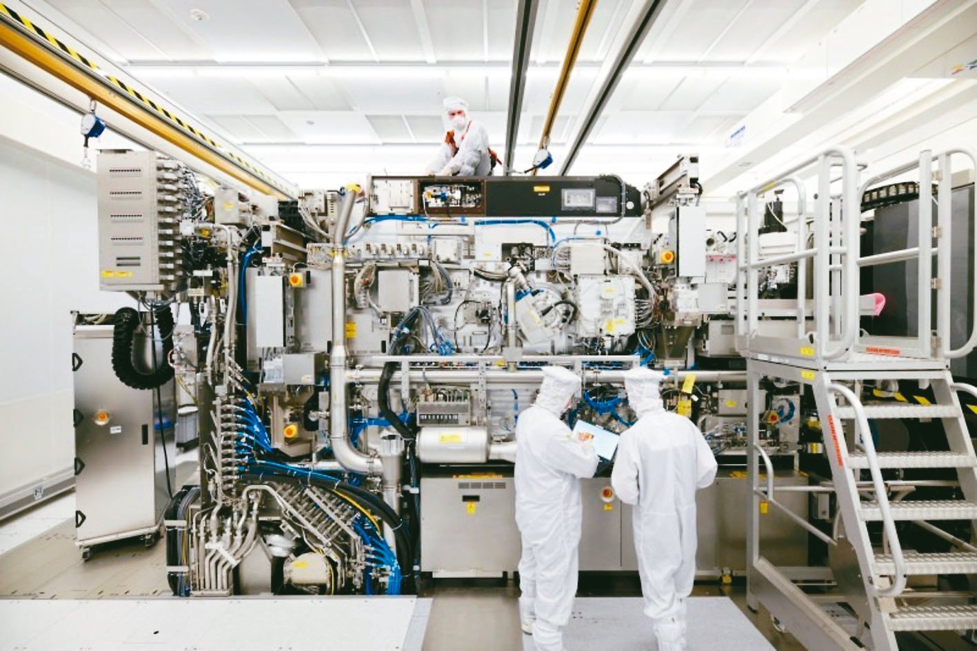
Once delivered to a wafer fab, a lithography machine is far from plug-and-play. It requires a lengthy “tuning” period—typically 6 to 12 months from uncrating to stable mass production. Even ASML’s mature EUV systems must be fully disassembled, reassembled, and calibrated to nanoscale precision upon arrival at the customer site. Veteran engineers note that achieving satisfactory wafer yield can take up to a year. For UEA’s domestic DUV, the challenge is even greater: it’s not just hardware validation but a full-chain ecosystem alignment.
1. Hardware Tuning: The “Physical Limit” at Nanoscale
A lithography machine is the pinnacle of human engineering, comprising hundreds of thousands of components where every micro-movement affects the whole. Post-assembly, the first step is level calibration: the platform must achieve nanoscale accuracy; otherwise, lens focus deviation distorts patterns. Testing occurs in two phases: at the factory, a “golden machine” serves as the benchmark, exposing wafers with standard masks featuring 90nm, 45nm, and 28nm patterns for result comparison. At the customer site, the process repeats, but the benchmark shifts to the fab’s existing DUV/EUV tools. Any deviation triggers iterative debugging—explaining the need for multiple prototypes in parallel: if one fails, others provide reference.
2. Environmental Factors: The Invisible “Yield Killers”
Precision instruments are hypersensitive to the environment; subtle fab changes can spell disaster. A classic case is an Intel fab where yield mysteriously dropped every dawn. Investigation revealed methane emissions (colloquially “cow farts”) from an upwind dairy farm reacting with process chemicals, disrupting lithography. Intel eventually paid to relocate the ranch. Similarly, TSMC’s U.S. F21 fab faced a “water droplet crisis”: within two hours of equipment restart, wafers showed defects. The culprit? Five water droplets that settled on a photoresist layer during downtime, causing nanometer-scale swelling and pattern deformation. The issue vanished once the droplets evaporated. These are not urban legends but warnings about environmental control. For UEA’s DUV, fab-specific climate, air pressure, vibrations, or nearby ranches can amplify yield fluctuations. China’s factories, often in industrial clusters, must counter these “invisible killers” via customized environmental simulations.
3. Software Tuning: The “Digital Magic” of Computational Lithography
No matter how precise the hardware, light remains “cunning.” At DUV wavelengths around 193nm, diffraction and interference through the mask turn right angles into curves and edges into zigzags, distorting patterns. This is where computational lithography steps in: algorithms simulate distortions, pre-applying “inverse deformations” on the mask—intentionally warping patterns to counteract physical effects. Additionally, “assistant features” are added: tiny sub-resolution patterns that don’t print but enhance contrast, sharpening main circuit contours.
UEA’s pain point is software independence: it cannot copy ASML code and, under U.S. export controls, lacks access to updates. In 2025, Chinese teams are accelerating native algorithm development, combining electromagnetic physics and iterative optimization, expected to take months to match global standards.
The U.S.-China Rivalry’s “Time Window”: Undercurrents Beneath a Truce
At the 2025 APEC Summit in Busan, South Korea, U.S. President Trump and Chinese President Xi Jinping’s meeting brought brief respite: China paused rare-earth export curbs, the U.S. resumed soybean purchases, and both cut tariffs by 10%. This is seen as a “mutual delay” strategy—trading chips to buy time for fixing weaknesses. Yet core issues remain untouched: U.S.-Japan-Netherlands export bans on high-end semiconductor equipment (e.g., EUV) persist, with only temporary buffers on controls.
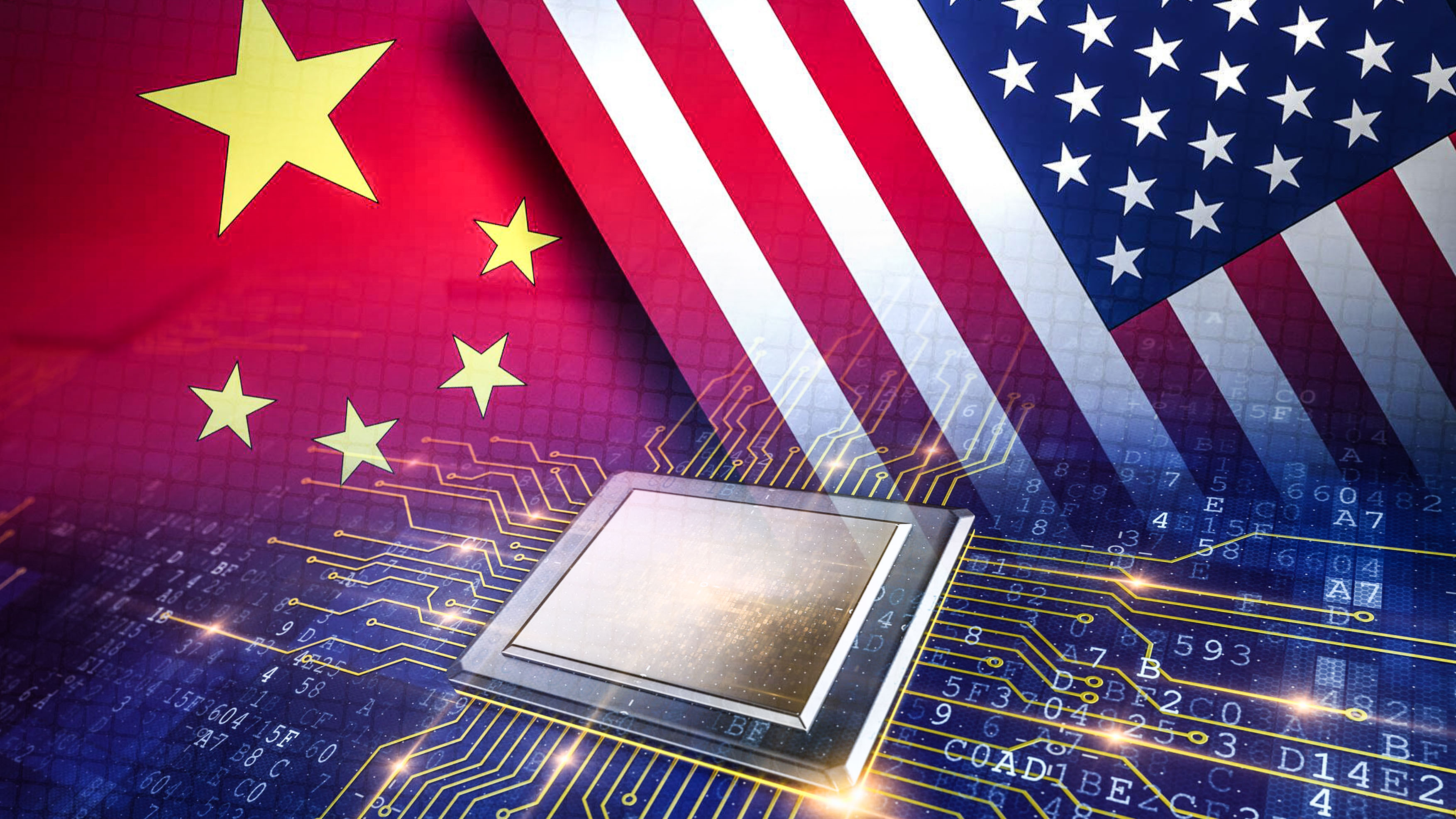
Does China still have time? The answer is yes. UEA’s DUV tuning is squarely within this window: through parallel prototypes and native software iteration, 28nm mass production is projected for early 2026. The U.S.-China competition won’t pause, but this is precisely the opportunity for self-reliance—from tuning one prototype to forging an industrial backbone, China’s semiconductor sector is writing its own Moore’s Law with precision and resilience.