Abstract
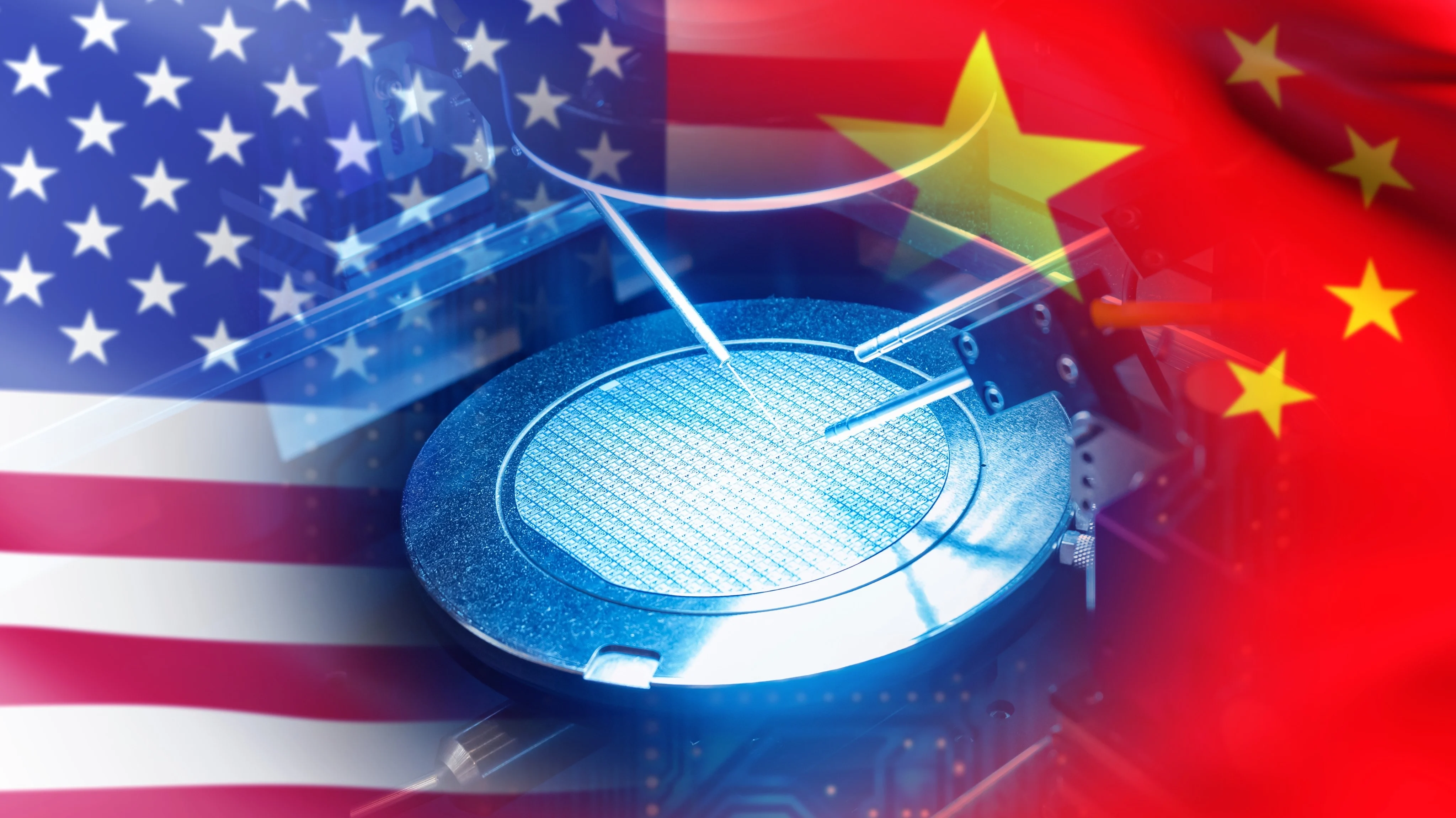
The autumn of 2025 witnessed a profound paradigm shift in the US-China technology conflict. Beijing launched a precise strike against the global semiconductor industry’s core vulnerability, particularly the Taiwan Semiconductor Manufacturing Company (TSMC), through an announcement utilizing the principle of extraterritorial jurisdiction (“long-arm jurisdiction”) over rare earth materials. The confidence behind this counterattack stems from China’s strategic breakthrough in domestic high-end lithography technology—an “Asymmetric Lithography” approach centered on AI-powered computation. This move signals China’s transition from passive defense to active offense. It also declares the end of the globalization era dependent on a single technological system, accelerating the world’s shift toward a dual-ecosystem competition where technology and geopolitics are deeply intertwined.

I. The “Achilles’ Heel” of Advanced Chip Manufacturing: The Indispensability of Rare Earths
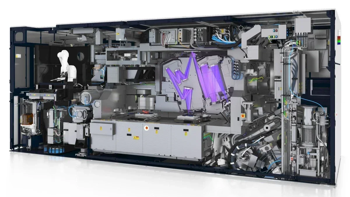
For a long time, the chip war narrative has focused on cutting-edge equipment like Extreme Ultraviolet (EUV) lithography machines. However, the recent crisis highlighted a severely underestimated factor: the absolute control that high-purity rare earth materials exert over the advanced chip fabrication process. The heart of global digital civilization—wafer fabrication—is critically dependent on rare earths in three key stages:
1. Core Abrasive for Chemical Mechanical Planarization (CMP)
Semiconductor manufacturing is akin to constructing a skyscraper with atomic precision, where the surface of every circuit layer must be mirror-smooth before etching, with deviations no greater than a single atomic layer. The critical enabler for this precision is the CMP slurry, whose core abrasive is high-purity, particle-size-precise Cerium Oxide (CeO2).
- Strategic Vulnerability: Despite the wide distribution of rare earth minerals, over 90% of the global capacity for refining, processing, and purifying high-purity Cerium Oxide is concentrated in China. An interruption in this supply would make it impossible to achieve the required nanometer-level flatness of the wafer surface, causing subsequent lithography focus to fail and effectively paralyzing chip fabrication.
2. The Driving Skeleton of Precision Equipment: Permanent Magnets
The highly automated, lightning-fast, and nanometer-precise positioning equipment in fabs like TSMC (including the dual wafer stages of lithography machines, vacuum pumps, robotic arms, etc.) requires powerful magnetic drive systems.
- Rare Earth Application: These systems rely on high-performance rare earth permanent magnets, primarily Neodymium-Iron-Boron (NdFeB). This strong magnet is the heart of all high-end manufacturing tools. Without it, capital equipment worth hundreds of millions of dollars loses its “muscle and nerves.”

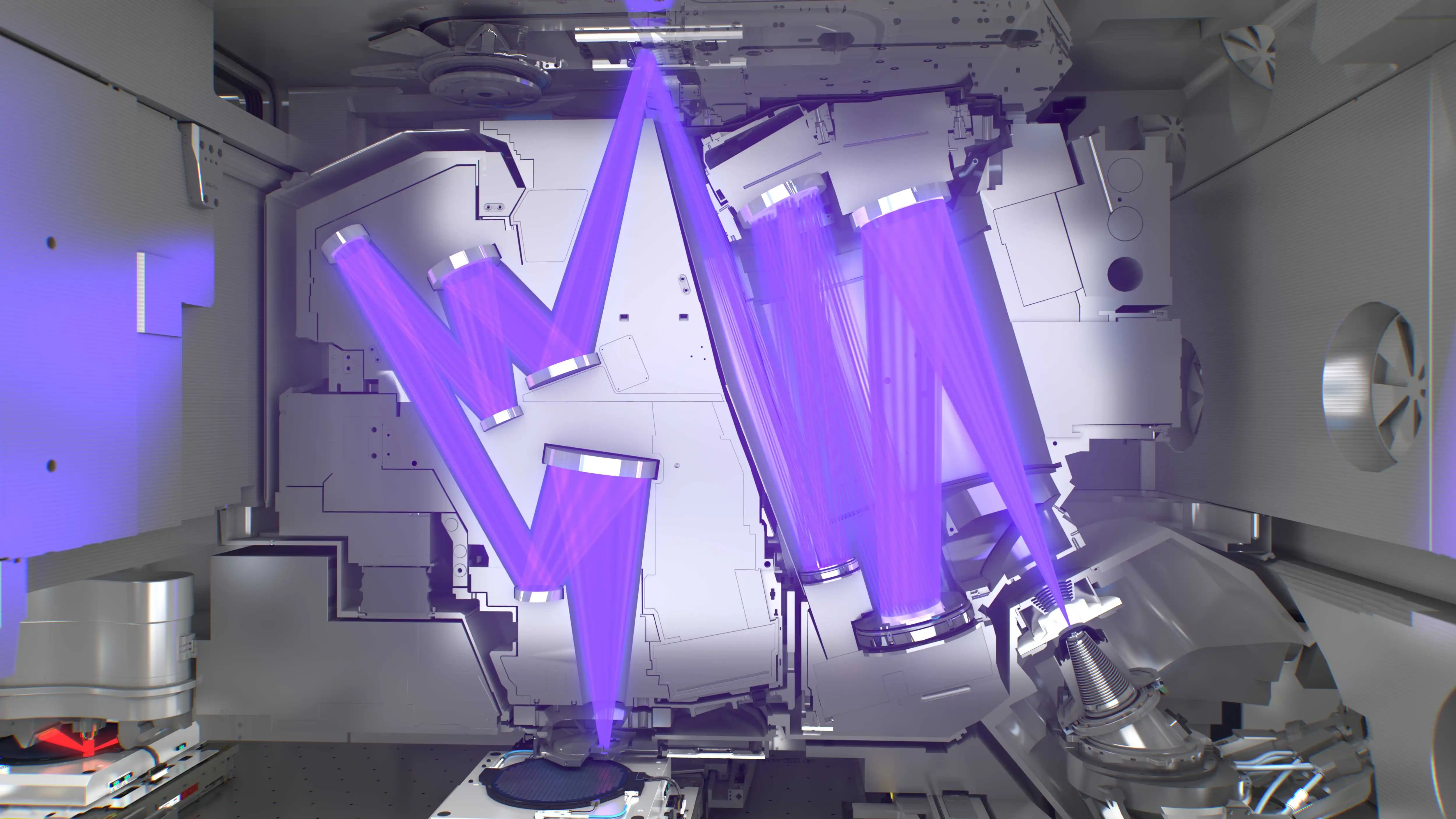
3. Chemical Medium for Cutting-Edge Lithography: EUV Photoresists
In state-of-the-art EUV lithography, the photoresist must efficiently absorb the Extreme Ultraviolet light with a mere 13.5 nm wavelength.
- Rare Earth Application: To enhance absorption efficiency and pattern fidelity, the photoresist requires sensitizers containing rare earth elements, such as Europium (Eu) and Terbium (Tb), which directly determines the yield and manufacturability of 7 nm and smaller chips.
China’s exercise of rare earth long-arm jurisdiction, notably requiring the tracing of even a 0.1% rare earth component value, ingeniously places an insurmountable compliance burden on the global supply chain. This forces technology suppliers worldwide to choose between complying with US sanctions and maintaining the stability of their supply chains, thus strategically dismantling the “Chip Alliance.”
II. Asymmetric Lithography: The Leap from Catch-Up to Overtake
China’s confidence in employing the “nuclear option” of rare earths stems from its domestic lithography technology achieving a level of “strategic self-reliance.” This breakthrough is not a simple replication of ASML’s technology but the forging of an innovative, asymmetric technological path, best described as “using mathematics to compensate for the limitations of physics.”
1. Physical Limits and the ASML Path
ASML’s EUV lithography machine represents the zenith of human precision engineering. Its strategy is governed by physical laws: enhance resolution by shortening the light’s wavelength from Deep Ultraviolet (DUV, 193 nm) to Extreme Ultraviolet (EUV, 13.5 nm). This is an extremely costly, complex, and protracted endeavor.
2. China’s Asymmetric Path: AI-Powered Computational Lithography
The Chinese team chose a computational-centric bypass route:
-
Technical Core: Integrating mature 193 nm DUV lithography machines with high-performance computing and Artificial Intelligence, specifically Computational Lithography (CL), and more profoundly, Inverse Lithography Technology (ILT).
-
Working Principle: Traditional lithography predicts the outcome of light projection. ILT reverses the calculation: What should the mask pattern look like to achieve the desired perfect nanometer-scale feature on the wafer?
-
AI Enablement: Historically, the sheer volume of computation for ILT was practically impossible in real-time. However, with the explosive development of GPU computing power and physics-informed deep learning models, Chinese teams have increased the computational efficiency by several orders of magnitude. This allows a DUV machine, operating at a fixed physical wavelength, to pre-compensate for all optical distortions through massive calculation, stably etching lines at 28 nm and even finer resolutions, far exceeding its theoretical limit.
-
Strategic Value: This “software-defined hardware” approach enables China to achieve “N-1” or “near-7 nm” performance without relying on ASML’s most advanced EUV equipment. This capability ensures that core defense and industrial production can be maintained even under extreme external blockade.
3. The Industrial Cornerstone Significance of 28 nm
The 28 nm node is regarded as the “Golden Node” of the semiconductor industry, serving as the manufacturing foundation for most critical industrial and civilian applications, including automotive electronics, industrial control, IoT devices, and communication base stations. The ability to mass-produce domestic 28 nm lithography machines means China has solved the “existence problem” of chips for core industrial sectors, building a solid strategic defense bulwark.
III. The Accelerated Restructuring of the Global Tech Ecosystem
The rare earth counterattack and lithography breakthrough are collectively driving the rapid restructuring of the global tech ecosystem, evident in two major developments:
1. ASML’s “Strategic Schizophrenia”
As the epitome of a technologically neutral supplier, ASML finds itself in an extremely awkward position. Its EUV technological “soul” is restricted by the US (core light source modules from a US subsidiary), while its commercial “body” increasingly relies on the Chinese market (where revenue share briefly surged). China’s rare earth long-arm jurisdiction, theoretically requiring ASML to obtain Chinese Ministry of Commerce permission for exporting lithography machines globally (as their components contain Chinese rare earth materials), subjects ASML’s worldwide operations to a dual squeeze and infinite compliance risk.

2. Huawei: Ecosystem Leader and Validator
Huawei’s “fight for survival” under US sanctions has positioned it as the “chain leader” and primary validation platform for China’s new semiconductor system.
-
Role Change: Huawei deployed engineering teams directly into domestic equipment vendors (like Shanghai Micro Electronics Equipment, SMEE), defining equipment technical specifications based on end-user needs and accelerating the industrialization of the domestic 28 nm DUV lithography machine.
-
Strategic Goal: Huawei’s roadmap for Ascend AI chips, for instance, indicates a strategy of leveraging advanced packaging and innovative chip architecture design to achieve performance leaps on “accessible process nodes,” thereby establishing complete independence from the Western technology framework.
Conclusion
The tech showdown of autumn 2025 signals that the focus of US-China competition has shifted from “who can make the most advanced chips” to “who can define and control the rules and standards for making chips.” The weaponization of rare earths and the maturity of asymmetric lithography have collectively ended the era of globalization dominated by a single technological hegemon.
The world is fragmenting into two parallel and competing ecosystems: one US-led, based on technological sanctions and alliances (like the exclusionary clauses of the CHIPS and Science Act); and the other China-centric, based on internal circulation, indigenous innovation, and asymmetric advantages (rare earths, computational lithography). For nations unwilling to align with either side, the Chinese technology ecosystem offers a “Plan B” devoid of political preconditions, which is poised to reshape the geopolitical and industrial landscape for decades to come. The grand duel over core technological sovereignty has just begun.