Amid escalating geopolitical tensions in the global semiconductor industry, China is rapidly advancing the localization of critical equipment like lithography machines. In September 2025, the Financial Times reported that Semiconductor Manufacturing International Corporation (SMIC) has begun testing China’s first domestically produced immersion deep ultraviolet (DUV) lithography machine, developed by Shanghai-based startup Yuliangsheng Technology (abbreviated as UEA).
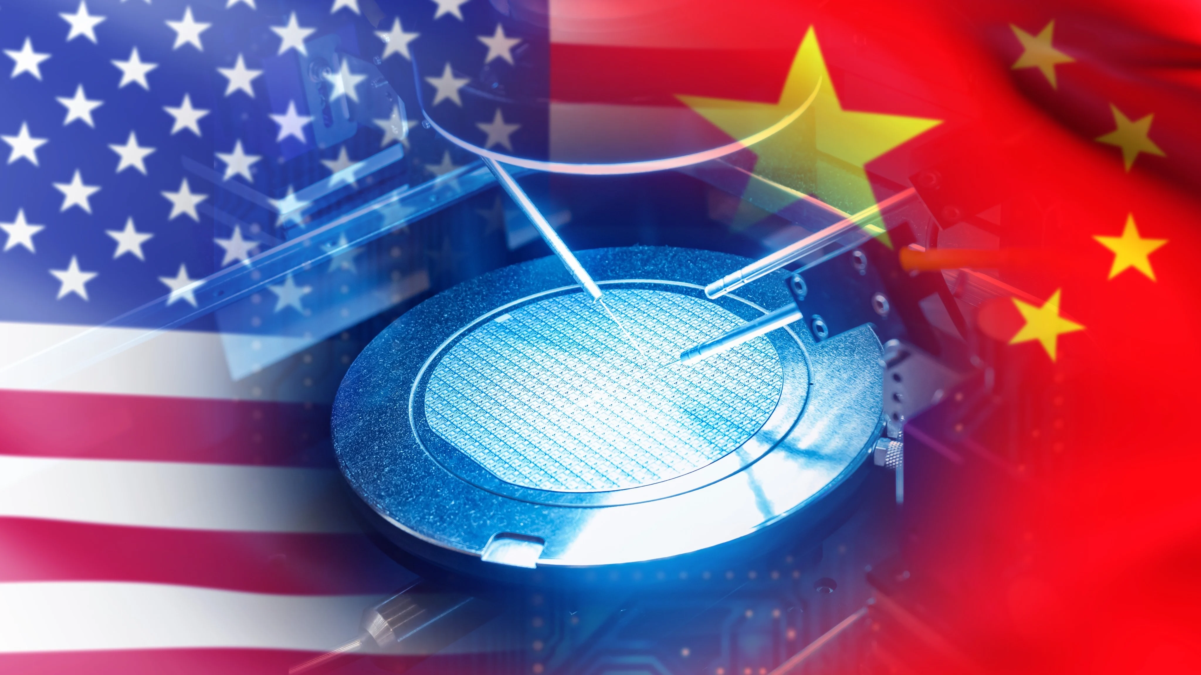
This milestone marks a significant step in mature and advanced chip manufacturing. Meanwhile, companies like Huawei and SiCarrier are accelerating extreme ultraviolet (EUV) lithography development to break Dutch firm ASML’s monopoly. Despite ongoing U.S. export controls, China’s long-term “02 Special Project” (initiated around 2008) has shifted the nation from “follower” to “challenger,” with domestic DUV expected for small-scale production by 2026 and EUV trials slated for Q3 2025.
DUV Lithography Progress: From Mid-to-Low End to High-End Immersion, Building Mature Process Foundations
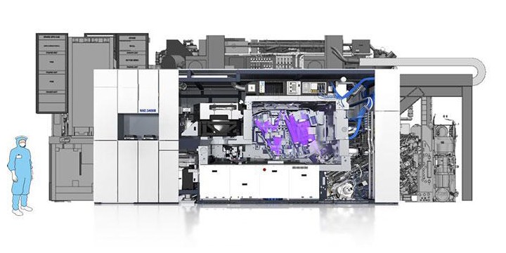
DUV lithography machines are core to semiconductor fabrication, using 193nm or 248nm laser wavelengths for pattern transfer. China’s breakthroughs stem from the national “02 Special Project” (full name: “National Major Science and Technology Project for Very Large Scale Integrated Circuit Manufacturing Equipment and Complete Processes”), launched in 2008 with billions in funding, focusing on full-chain R&D from light sources to integrated systems. By 2025, the project has spawned firms like Shanghai Micro Electronics Equipment (SMEE) and UEA, advancing domestic DUV from 90nm to 28nm.
Mid-to-Low End DUV: Standardized Promotion of KrF and ArF The 2024 edition of the Ministry of Industry and Information Technology’s (MIIT) “Guidelines for the Promotion and Application of the First Set of Major Technological Equipment” explicitly lists KrF (krypton fluoride, 248nm) and ArF (argon fluoride, 193nm) DUV equipment, supporting mature processes above 65nm. These are akin to “luxury sedans” like BMWs, ideal for automotive electronics, IoT, and consumer chips. SMEE’s SSA600 series has achieved 90nm resolution mass production, with the 2023 SSA800 series improving to 65nm, delivered to multiple fabs. Per SEMI data, China’s 2025 wafer fab expansion will add three new facilities, nearing 50 total, surging demand for mid-to-low end DUV with annual sales projected in the hundreds.
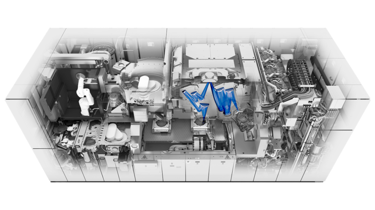
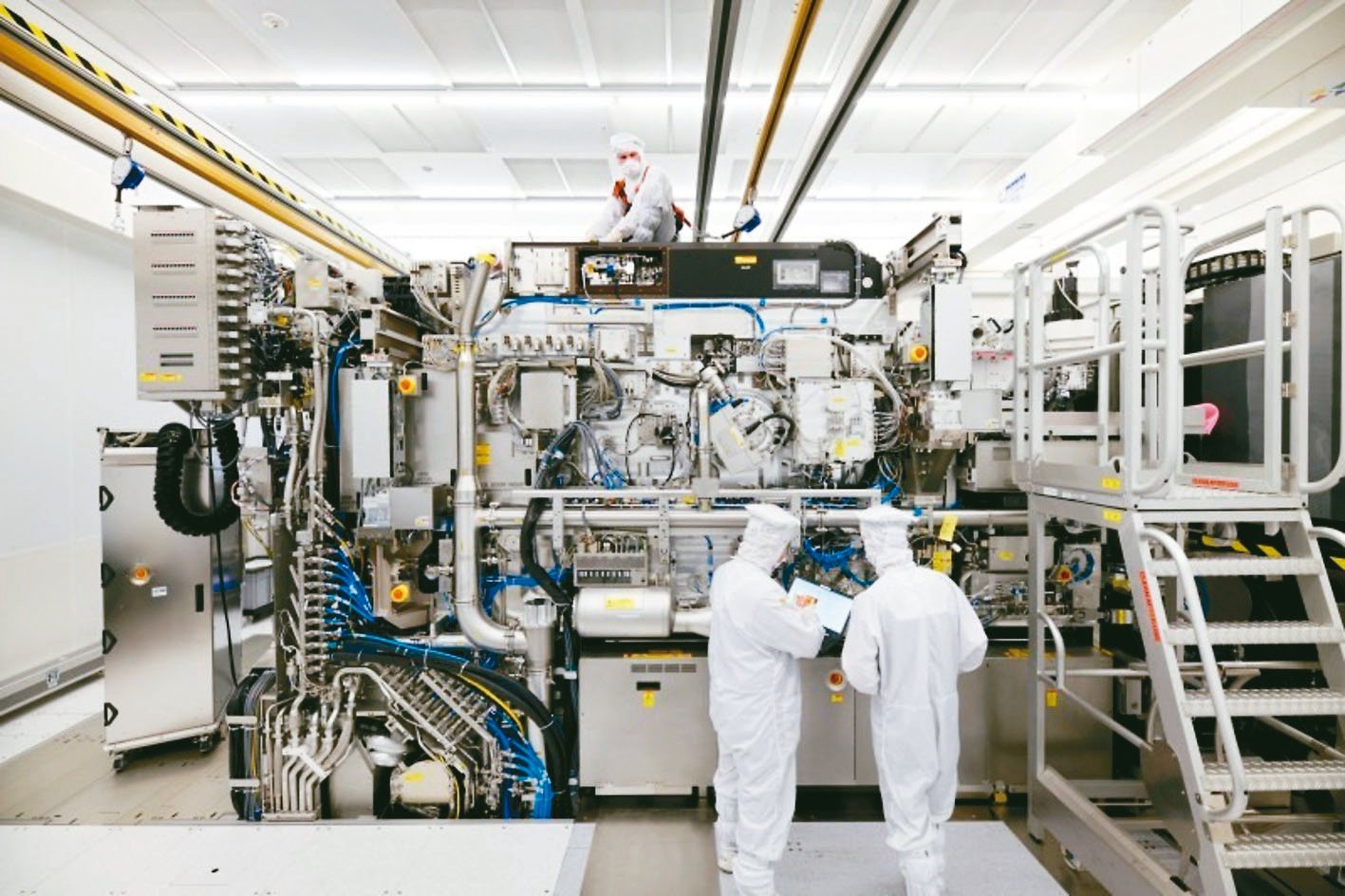
High-End Immersion DUV (ArFi): Line Debugging, Challenging 7nm Nodes The pinnacle of DUV is ArFi (immersion ArF), injecting water between the lens and wafer to boost numerical aperture (NA) above 1.35, achieving 38nm resolution. In 2025, UEA’s prototype is undergoing debugging at SMIC’s Southern Epoch fab in Shanghai (SMSC), with promising initial results. This “Porsche-level” tool is mostly domestically sourced, with only minor optics imported. Paired with self-aligned quadruple patterning (SAQP), it can reach 5nm nodes.
SAQP requires 4-5 exposure layers, doubling or tripling complexity versus ASML’s single-exposure EUV, dropping yields from TSMC’s 85% to 30%-50% and raising wafer costs 40%-50%. Nonetheless, SMIC has used stockpiled ASML DUV for 7nm production, powering Huawei’s Ascend AI chips. Line integration is eyed for early 2026, small-scale production in 2027, lifting localization from 30% to 70%. Markets reacted bullishly: On September 17, SMIC’s A-shares surged 10%, lifting SMEE to limit-up.
Transistor Architecture Optimization: Evolving from FinFET to GAAFET/CFET To maximize DUV potential, Chinese firms are refining transistor structures. Transitioning from FinFET to GAAFET (gate-all-around) and CFET (complementary FET) could push nodes to 3nm or 2nm. Huawei unveiled 31 tools at SEMICON China 2025, supporting 5nm GAAFET processes. Tsinghua University and the Changchun Institute of Optics’ poly-telluroxane (PTeO) resist achieves 0.02nm wavefront distortion for enhanced resolution. Yet, iterations face thermal and parasitic challenges, needing 3-5 years.
EUV Lithography Outlook: Light Source and Integration Hurdles, Trials Eyed for 2025
EUV is essential for sub-7nm nodes, using 13.5nm wavelength reflective mirrors for single exposure. The “02 Special Project” has reserved EUV tech since 2008, including sources and optics. In 2025, China’s EUV efforts hit stride, with SiCarrier’s “Mount Everest” project targeting commercialization by 2026.
Light Source Paths: LDP vs. LPP ASML’s laser-produced plasma (LPP) hits tin droplets with high-power CO2 lasers, yielding 2%-5% efficiency at 250W. China favors laser-induced discharge plasma (LDP), vaporizing tin via high-voltage discharge for 2.3% efficiency, shrinking size 30% and costs 45%. The first LDP prototype tested at Huawei’s Dongguan fab in March 2025, at 50W for 5-3nm nodes, but throughput is just 10 wafers/hour (vs. ASML’s 150). Harbin Institute of Technology’s Zhao Yongpeng team stabilized 13.5nm output.
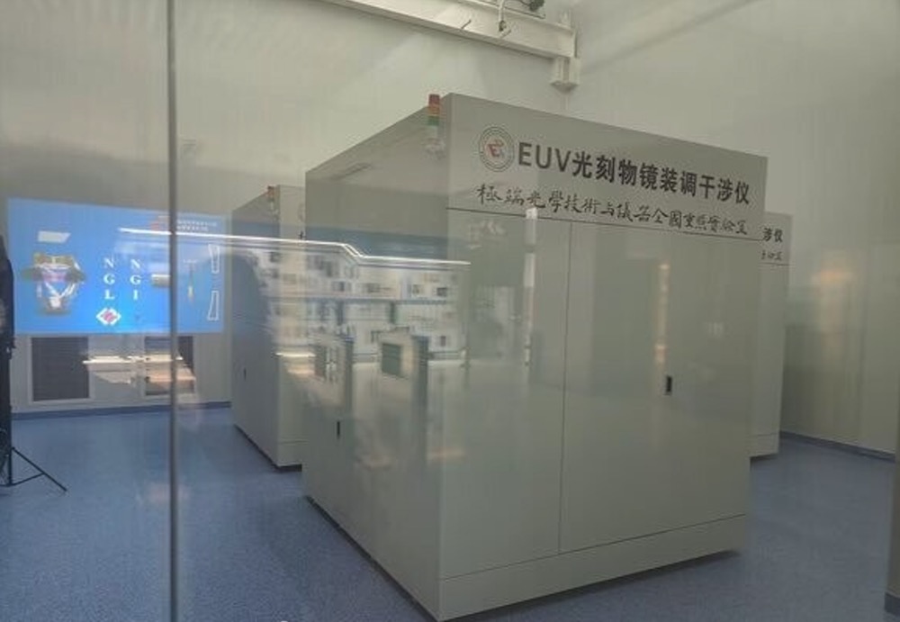
Integration Challenges: From Components to Systems EUV’s crux is integrating 100,000+ parts at picometer precision. SMEE’s 2023 patents cover EUV generators and tools, while Tsinghua’s SSMB-EUV builds test platforms. Q3 2025 trials are planned, with Hyperion-2 (150W) in 2026 yielding 80%. Phase III Big Fund ($47.5B) backs sub-10nm localization by 2030.
Conclusion: National Resolve Forges Resilience, the Long Road to Demystifying ASML
Years of tech controls have failed to halt China, much like successes in CR450 high-speed rail and Dongfeng 5C missiles. DUV paths are nearly complete, EUV the next 2-3 years’ focus. With 50 fabs expanding, this ecosystem will redefine globals. Yield/cost bottlenecks persist, but via patents (SiCarrier: 800+) and talent, 100% self-sufficiency by 2030 is the goal. Semiconductor autonomy is tech race and national imperative—prospects shine.