As the global semiconductor industry navigates intense competition, China is accelerating its push for domestic lithography technology, the cornerstone of chip manufacturing. Amid ASML’s dominance and US export controls, Chinese firms are pursuing parallel paths: Shanghai-based Yuliang Sheng (UEA) excels in DUV technology, rapidly validating advanced nodes, while Shenzhen SiCarrier, in collaboration with Huawei, bets on innovative EUV solutions. SiCarrier’s planned 5nm trial production in Q3 2025 has gone quiet, likely due to technical bottlenecks, but this is a stepping stone, not a dead end. This article examines UEA’s progress, contrasts SiCarrier’s challenges, analyzes technical strategies, and explores China’s semiconductor future.
UEA’s DUV Breakthrough: Midcore Validates 5nm Potential
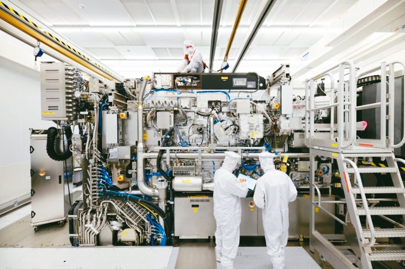
Shanghai’s Yuliang Sheng (UEA) is emerging as a frontrunner in China’s lithography race. On September 17, 2025, the Financial Times reported that Midcore International began testing UEA’s first domestic deep ultraviolet (DUV) lithography machine. This milestone signals China’s progress toward self-reliant advanced semiconductor equipment, targeting 5nm processes.UEA’s DUV system, inspired by ASML’s immersion technology, leverages multiple patterning (e.g., SAQP) to achieve advanced nodes.
With most components domestically sourced and only select critical parts imported, it achieves an overlay accuracy of 1.3nm, surpassing the 1.4nm threshold for 5nm processes. Early tests show promise, with Midcore’s involvement confirming compatibility. If successful, this could save hundreds of millions annually in chip procurement costs. The breakthrough boosted A-share lithography stocks, with Wavelength Opto-Electronic up nearly 18% and Yongxin Optics hitting a 10% cap. On X, Japanese users hailed it as “China’s first domestic advanced semiconductor tool.”
SiCarrier’s 5nm Trial Stalls: Q3 Silence Signals Bottlenecks
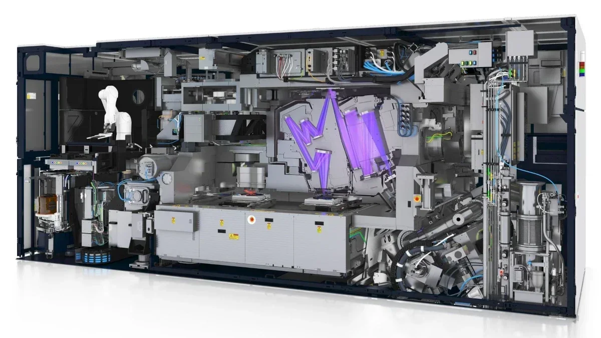
In contrast, Shenzhen-based SiCarrier, backed by state-owned capital, pursues an ambitious EUV path. With a core team from Huawei, SiCarrier unveiled 31 “Famous Mountain” tools at SEMICON China 2025, supporting 5-28nm processes. It planned 5nm trial production in Q3 2025 at Huawei’s Dongguan factory in Songshan Lake, near Shenzhen, using LDP (Laser-induced Discharge Plasma) to generate a 13.5nm EUV light source.
Yet, as Q3 ends, updates are scarce. Discussions on Zhihu and X question why “SiCarrier’s 5nm remains elusive.” Leaked photos from Huawei’s Songshan Lake factory in Dongguan—a sprawling R&D hub styled like a European town—show an EUV machine labeled “Made in China” operating in a cleanroom. These images are likely authentic, given Songshan Lake’s role as Huawei’s innovation center. The delay stems from immature processes, with LDP light source power as the primary bottleneck. LDP generates 13.5nm light via high-voltage discharge, offering 4.5% efficiency (vs. ASML’s 2%) and 30% lower costs. However, its output of 100-150W falls short of ASML’s 250W+, reducing exposure efficiency and yielding 33%-70%.
Shenzhen vs. Shanghai: R&D Strengths and Strategic Focus
SiCarrier’s setback doesn’t reflect Shenzhen’s inferiority. Huawei’s R&D hub in Songshan Lake, Dongguan, near Shenzhen, boasts superior innovation capacity compared to Shanghai, with facilities like the Spallation Neutron Source. While lacking a foundry like Midcore, Shenzhen bridges this gap through Huawei’s collaboration with SMIC on chips like Kirin. SiCarrier’s 28nm immersion lithography tool, SSA800i, achieves <2nm overlay accuracy in lab tests.UEA’s DUV approach, while effective, closely mirrors ASML, limiting long-term innovation. SiCarrier’s LDP path avoids patent barriers, offering a disruptive alternative. Huawei’s 20 billion yuan investment bolsters SiCarrier’s persistence.
LDP Power Bottleneck: An Engineering Challenge, Not a Scientific Barrier
LDP’s power shortfall is a significant but solvable issue. The challenge lies in optimizing tin vapor conversion efficiency through precise high-voltage discharge control. Collaborative research by Harbin Institute of Technology and the Chinese Academy of Sciences has doubled efficiency, with further gains expected via algorithms and material upgrades. Huawei’s patents, such as CN202110524685X, target EUV light source innovation. From lab to production, Shenzhen’s process can cut cycles by 30%, with power breakthroughs anticipated by late 2025, potentially pushing 5nm yields above 80%.
Dual-Track Strategy: Short-Term Stability, Long-Term Ambition
China’s dual-track lithography strategy balances immediate needs with future goals. UEA’s DUV systems enhance 7nm+ chip capabilities, improving yields and stabilizing computing power through advanced packaging like 3D IC. This buys time for EUV development, with China holding a 34.4% share of the $330 billion global semiconductor equipment market in 2025. ASML’s 36.1% China revenue underscores the urgency of domestic alternatives. SiCarrier’s EUV efforts, paired with UEA’s DUV, form a robust ecosystem, with Huawei’s Mate series potentially debuting a 5nm Kirin chip.
Conclusion: A Measured Path to Lithography Independence
UEA’s DUV testing and SiCarrier’s EUV challenges highlight China’s multifaceted approach to lithography self-reliance. While SiCarrier’s LDP power issues delay 5nm trials, they are engineering hurdles, not insurmountable barriers. Shenzhen’s R&D prowess, bolstered by Huawei-SMIC collaboration, complements UEA’s rapid DUV progress. This dual strategy ensures short-term chip supply stability and long-term innovation, positioning China to reshape the global semiconductor landscape through steady, calculated advances.