Here is a detailed outline of the topics discussed:
Part 1: Electronic Design Automation (EDA)
-
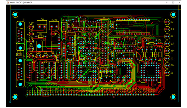
What is EDA? The video defines EDA as a set of computer-aided design tools and software used to design integrated circuits (ICs).
-
The Importance of EDA: It explains that with billions of transistors on a single chip, manual design is impossible, making EDA crucial for efficiency and accuracy.
-
EDA Functions: EDA tools aid in creating circuit layouts and perform simulations to verify the IC’s functionality, performance, and heat dissipation.
-
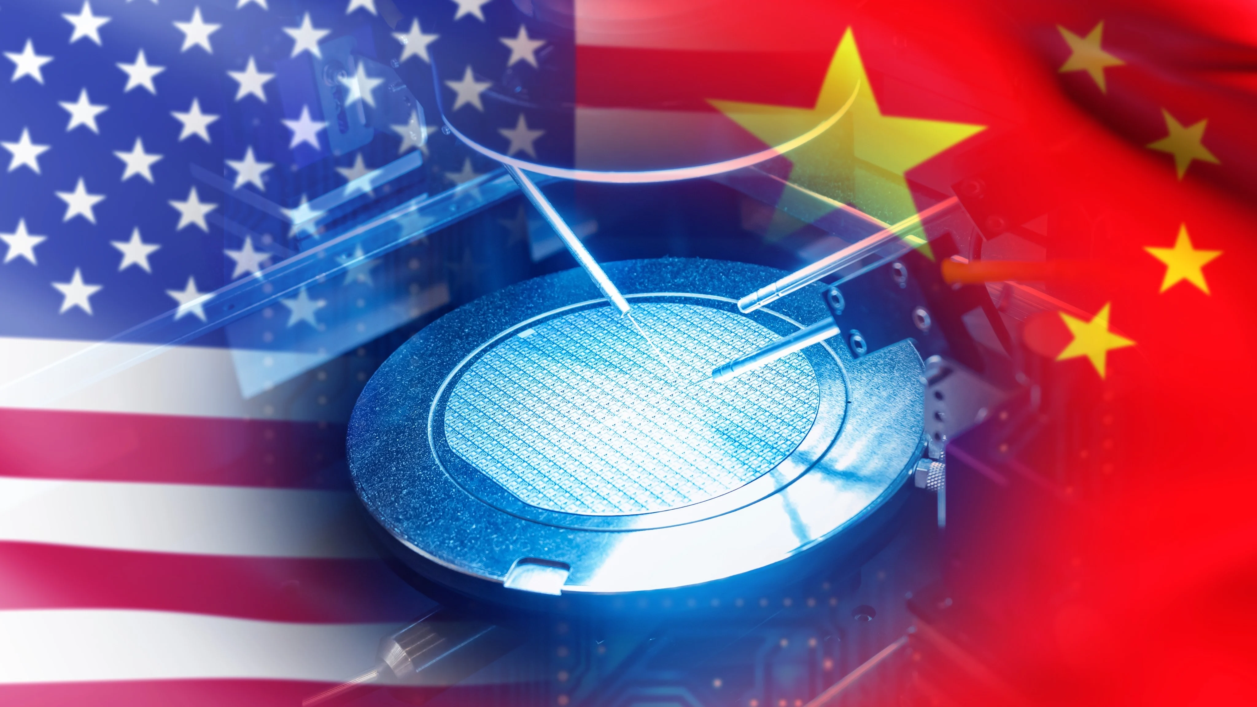
Market Overview: The video highlights that US companies, namely Synopsys, Cadence, and Siemens, dominate 70-80% of the global EDA market. It contrasts this with Chinese EDA companies, which have less than 20 years of experience and are limited to mature 28nm processes and above.
-
US Sanctions: The video mentions that the US export ban on advanced EDA tools, specifically for GAAFET below 3nm, has effectively halted China’s progress in advanced chip manufacturing.
Part 2: Transistors and Lithography
-
Transistor Basics: The video explains how transistors act as electrical switches on an IC.
-
Moore’s Law: It discusses Moore’s Law, which predicts the doubling of transistors on a chip approximately every 18 months, driving the need for smaller transistors.
-
Evolution of Transistor Structures:
-
The video introduces the early 2D planar transistor (planarFET).
-
It then explains the transition to 3D FinFET to solve leakage and overheating issues as transistors became smaller.
-
Finally, it introduces the next-generation Gate-All-Around (GAAFET) structure, which is necessary for processes below 3nm.
-
-
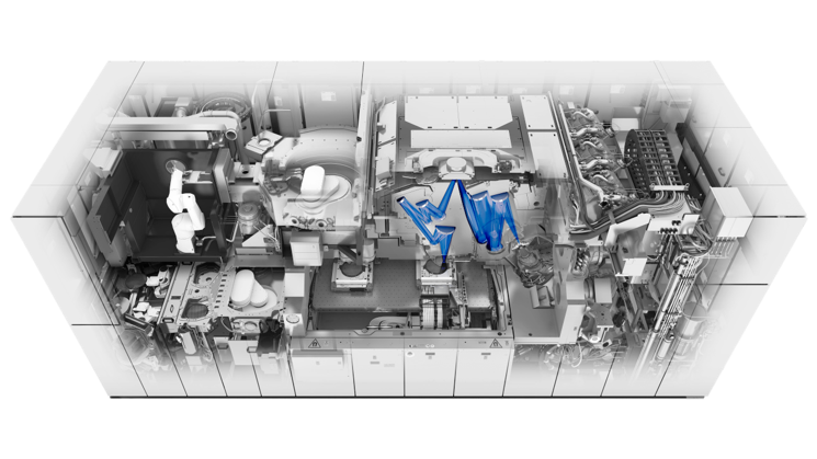
Photolithography: The video delves into photolithography, the process of etching circuit patterns onto a silicon wafer.
-
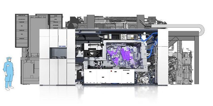
EUV Lithography:
-
It explains the key role of EUV (Extreme Ultraviolet) lithography machines, particularly those made by ASML, in advanced chip manufacturing.
-
The video details the five steps of the photolithography process: photoresist coating, exposure (with a mask), development, etching, and cleaning.
-
It highlights the importance of using a short light wavelength for higher resolution, which is why EUV’s 13.5nm wavelength is so crucial for fine line widths.
-
-
Multi-Patterning: The video explains that Chinese companies like SMIC have used DUV (Deep Ultraviolet) with multi-patterning techniques to achieve 7nm processes, but this method is more complex, costly, and yields lower quality compared to single-exposure EUV.
Part 3: Semiconductor Manufacturing and Supply Chain
-
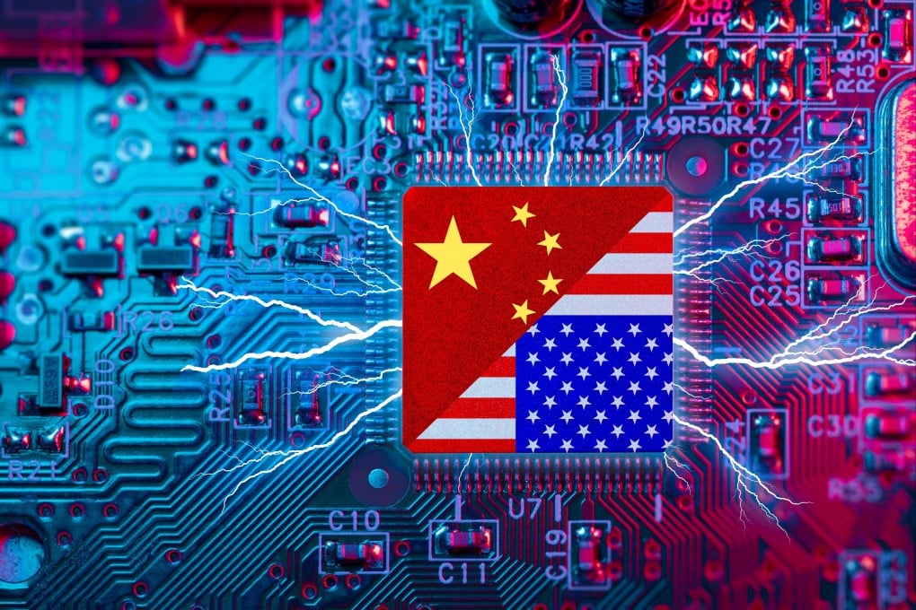
US Export Controls: The video discusses the US Commerce Department’s ban on exporting semiconductor manufacturing equipment for processes below 14nm to China, affecting key companies like Lam Research and Applied Materials.
-
Wafer Production: It describes the process of creating silicon wafers from sand, emphasizing the high purity required for advanced ICs and the dominance of Japanese suppliers like Shin-Etsu Chemical.
-
Key Manufacturing Steps: The video outlines the core steps of semiconductor fabrication:
-
Deposition: Growing thin films on the wafer surface.
-
Photolithography: Transferring circuit designs using light.
-
Etching: Removing unwanted material to form the circuit structure.
-
-
Role of Key Companies: The video explains why companies like Lam Research (etching/deposition), Applied Materials (deposition/inspection), and KLA (process control) were targeted by US sanctions, as they control critical parts of the manufacturing process.
Part 4: Advanced Packaging and Moore’s Law
-
Beyond Moore’s Law: The video discusses the concept of “More than Moore,” which focuses on improving chip performance without simply shrinking transistor size, often through advanced packaging.
-
Traditional Packaging: It outlines the basic steps of traditional chip packaging: dicing, die bonding, wire bonding, and molding.
-
Advanced Packaging: The video highlights advanced packaging techniques, particularly 3D stacking, which dramatically shortens the distance between dies, improving data transmission speed and reducing power consumption.
-
TSMC’s Role: It mentions TSMC’s 3D Fabric alliance and its CoWoS, InFO, and SoIC advanced packaging technologies, which are used in high-performance chips like Apple’s M-series.
Part 5: Thin Film Deposition Technology
-
Importance of Thin Films: The video explains that for advanced chips, the quality of the thin film layers is paramount, as they need to be uniform and only a few atoms thick.
-
Deposition Methods: It categorizes thin film deposition into physical and chemical methods, with Chemical Vapor Deposition (CVD) being a common chemical technique.
-
Atomic Layer Deposition (ALD): The video introduces ALD as a refined version of CVD that allows for precise, self-limiting deposition of single-atom layers, crucial for complex 3D structures.
-
ASML’s Leadership: It credits ASML’s sister company, ASM, as a leading provider of ALD equipment, playing a vital role in manufacturing advanced chips.
Part 6: CPU, GPU, and TPU: The Evolution of Computing
-
Von Neumann Architecture: The video explains the foundational Von Neumann architecture, which consists of memory, a control unit (CU), and an arithmetic logic unit (ALU), all central to the CPU.
-
CPU (Central Processing Unit): It describes the CPU’s role as a general-purpose processor that performs complex tasks sequentially, like a single production line.
-
GPU (Graphics Processing Unit): The video explains the shift to parallel processing with the GPU, which contains hundreds to thousands of ALUs. This makes it highly efficient for tasks with massive data, such as image processing.
-
TPU (Tensor Processing Unit): It introduces the TPU as a specialized chip designed for matrix calculations, a core component of AI and machine learning.
-
AlphaGo and Google’s Tensor Chip: The video uses the example of AlphaGo’s victory over Lee Sedol to demonstrate the power of TPUs. It concludes by discussing Google’s Tensor chip, which integrates a TPU for AI-specific tasks, and its application in products like the Pixel 7.