突破了什么?能实现量产吗?国产LDP EUV技术细节深入解析!")
The video provides an in-depth look at China’s advancements in Extreme Ultraviolet (EUV) lithography technology.
Here is a summary of the main points discussed:
-
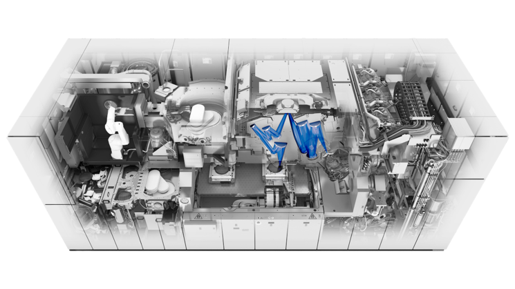
What is EUV Lithography? The video explains that EUV lithography, which uses a 13.5 nm wavelength, is crucial for producing advanced chips at 5 nm and below. It highlights the basic working principles of a lithography machine, from the precise positioning of the wafer to the exposure process that imprints circuit patterns.
-
Evolution of Lithography: It traces the history of lithography from early methods like contact and proximity lithography to the revolutionary scanning projection lithography that transformed the semiconductor industry.
-
EUV Light Source Technologies: The video delves into the complex process of creating EUV light. It contrasts the two main methods: Discharge-Produced Plasma (DPP) and Laser-Produced Plasma (LPP). The video notes that ASML, the current leader in EUV technology, chose the LPP path after acquiring its partner, Cymer.
-
Why LDP Technology Still Matters: Despite ASML’s decision, the video argues that Laser-Induced Discharge Plasma (LDP) technology is still relevant and holds significant promise for China’s semiconductor industry. It explains that LDP technology is scalable, can bypass patent barriers from ASML and its partners, and offers a viable path for achieving self-reliance in EUV source development.