This video discusses China’s recent developments in lithography technology, specifically focusing on two new products that have been launched by Chinese companies.
Key points include:
-
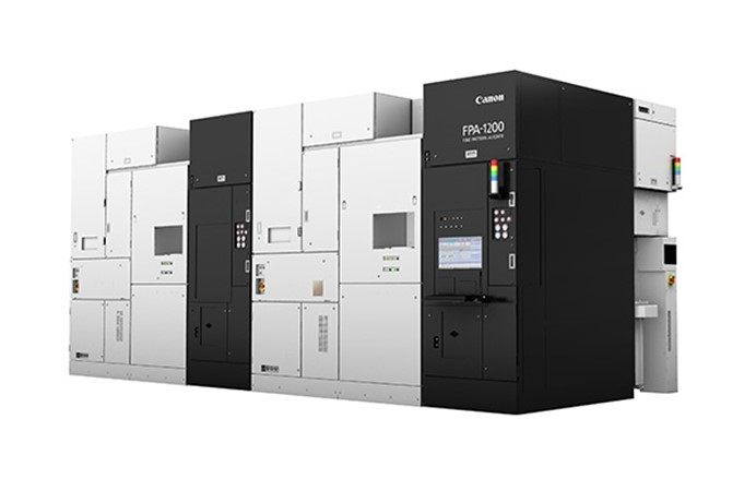
China’s struggle to obtain EUV lithography systems: The video explains that the US has restricted the export of advanced lithography equipment to China, which has prevented the country from acquiring EUV (Extreme Ultraviolet) lithography systems from ASML, the sole global manufacturer.
-
New Chinese lithography products: Two products are introduced:
- Nano-imprint equipment from PNO: This device, based on nano-imprint technology from the 1990s, was announced on August 8th and can produce electronic circuit patterns in the nanometer range. The video notes that while the technology has existed for a long time, it has not become a mainstream method for mass production due to issues like low production efficiency and alignment problems.
- Electron beam lithography machine from Hangzhou Chengxi: Announced on August 10th, this machine uses electron beam direct-writing technology, which has been in development since the 1960s. The video explains that this method is also unsuitable for mass production because it is extremely slow, taking up to a month to process a single wafer.
-
The products’ significance: The video concludes that although these new products are not viable alternatives to EUV for large-scale commercial production, they are significant milestones in China’s efforts to overcome US restrictions and advance its semiconductor capabilities. They represent an important step in China’s technological journey, even if they don’t immediately solve the country’s challenges in the semiconductor industry.