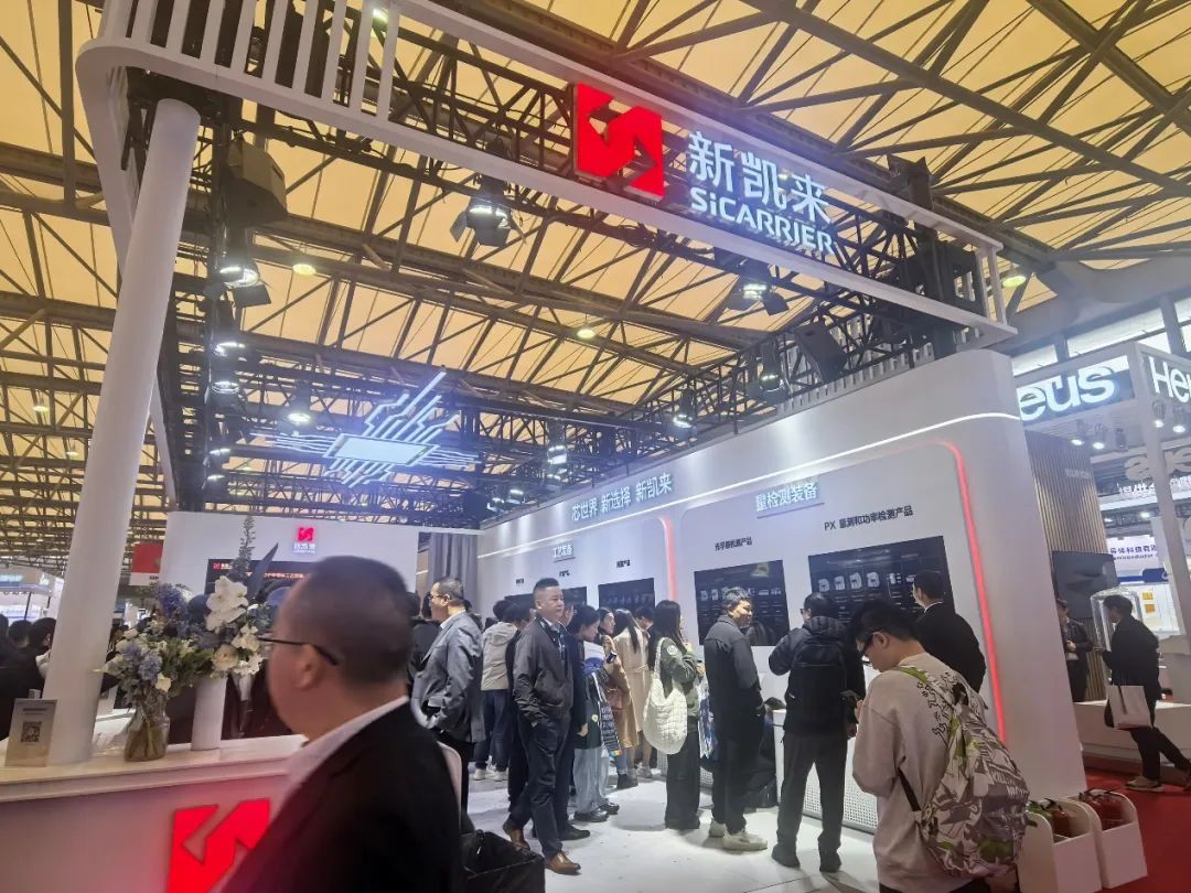
In September 2025, a groundbreaking development from Shanghai’s Pudong District reverberated through the global semiconductor industry: Shanghai UEA Technology Co., Ltd(宇量升 YuliangSheng). (UEA) successfully tested its deep ultraviolet (DUV) lithography machine on Semiconductor Manufacturing International Corporation’s (SMIC) Shanghai production line. This milestone marks a pivotal step in China’s quest for semiconductor self-reliance, moving critical “chokepoint” technology from the laboratory to real-world production. In just three years since its founding, UEA has emerged as a symbol of China’s technological ambition. This article explores UEA’s rise, its strategic significance in the chip supply chain, and the challenges and opportunities facing China’s semiconductor industry.
UEA: A Rising Star in Semiconductor Equipment
Shanghai UEA Technology Co., Ltd. was established in July 2022, headquartered at 500 Mindong Road, Pudong New District, with a registered capital of 1 billion yuan. Backed by state-owned capital, the company employs between 100 and 499 people, with over 90 percent dedicated to research and development. More than 60 percent of its workforce holds master’s or doctoral degrees. The founding team, a blend of overseas-trained experts and local talent, set out to tackle the core challenge of semiconductor equipment: lithography technology. This field, often called the “crown jewel” of chip manufacturing, has long been dominated by Dutch giant ASML, leaving Chinese firms dependent on foreign suppliers.
UEA operates with a modern, open research framework, emphasizing pragmatism, problem-solving, and collaboration. Unlike traditional state-owned enterprises, its culture resembles that of a Silicon Valley startup, with a young team and frequent cross-disciplinary partnerships. In 2025, UEA launched a high-profile campus recruitment drive, offering competitive salaries for master’s graduates, slightly above industry averages, along with opportunities like Shanghai’s selective civil service program. Job postings on platforms like BOSS Zhipin and Niuke cover roles in software development, precision optics, and algorithm optimization, attracting top talent in semiconductors and related fields. UEA’s appeal lies not just in compensation but in its mission to shape history.
DUV Breakthrough: From Lab to Production Line
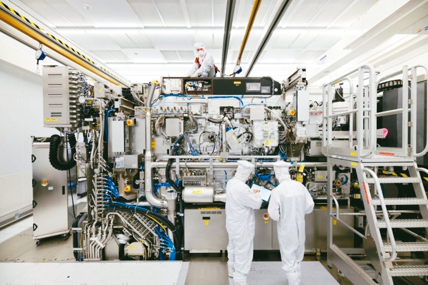
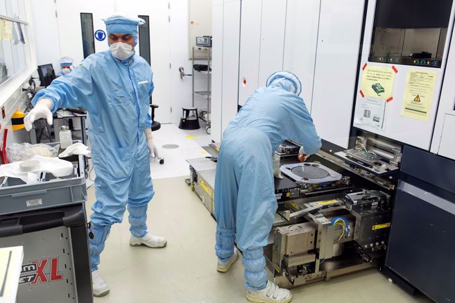
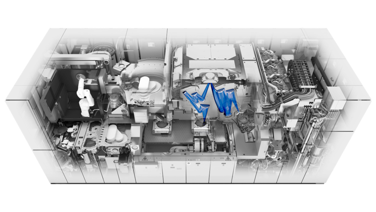
Lithography machines are the cornerstone of chip manufacturing, projecting circuit patterns onto silicon wafers. DUV lithography uses a 193-nanometer light source and immersion technology to support production at 28 nanometers and above. With multi-patterning techniques, where patterns are layered through multiple exposures, DUV systems can extend to 7 nanometers or even 5 nanometers, though with lower yields of around 30 to 40 percent.UEA’s DUV lithography machine, inspired by ASML’s TWINSCAN immersion systems, represents a leap forward. Most components, including the light source and lens systems, are domestically produced, with only precision optical lenses still reliant on imports. In September 2025, SMIC began testing this equipment on its Shanghai production line.
Initial results are promising, with stability meeting expectations for 28-nanometer production. Multi-patterning enables 7-nanometer processes, and in extreme cases, 5-nanometer attempts are feasible. This marks China’s first advanced DUV system to undergo production-line validation.The testing phase is a starting point, not an endpoint. The equipment requires at least one year of iteration to improve yield and reliability for large-scale production. UEA aims to achieve stable 7-nanometer production by 2027 while accelerating full supply chain localization to eliminate dependence on imported components like optical lenses. This breakthrough signals China’s transition from trailing to competing in semiconductor equipment.
Strategic Significance in the Chip Supply Chain
-
Filling the Supply Chain Gap
Export controls by the US, Netherlands, and Japan restrict ASML’s DUV lithography machines, requiring US approval for sales to Chinese firms, while extreme ultraviolet (EUV) systems are entirely banned. UEA’s DUV equipment offers a viable alternative for SMIC and other foundries, ensuring production of 28-nanometer and above chips. These nodes account for roughly 70 percent of global chip demand, covering applications in industrial control, automotive electronics, the Internet of Things, and AI chips. While not yet rivaling cutting-edge 3-nanometer processes, localized mature nodes secure China’s domestic supply chain. -
Building an Ecosystem
UEA’s progress catalyzes development across the supply chain. Domestic production of light sources, precision mechanics, and photoresists accelerates, forming a closed-loop ecosystem with SMIC and Huahong Semiconductor at its core. This reduces costs and lays the groundwork for future EUV research. -
Bridging the Gap with Stacking and Multi-Patterning
For 5-nanometer and below nodes, DUV systems can leverage multi-patterning and 3D stacking technologies, such as Chiplet architectures, to enhance performance and offset process limitations. This approach suits industrial and server chips, which prioritize reliability over extreme power efficiency. In the short term, UEA’s equipment can support China’s smart manufacturing and electric vehicle sectors, buying time for EUV development.
Challenges Facing China’s Semiconductor IndustryDespite UEA’s breakthrough, significant hurdles remain:
-
Technical Barriers
DUV systems need further optimization in yield and durability to match ASML’s mature equipment. EUV development, codenamed “Everest,” faces even greater complexity, involving 13.5-nanometer light sources and high-numerical-aperture lenses. Stable EUV production is unlikely before 2028. High-end materials like photoresists and ultra-pure gases also lag in localization. -
Global Competition and Restrictions
ASML and Nikon hold over 95 percent of the global lithography market, with rapid technological advancements. Tightening export controls by the US, Netherlands, and Japan may extend to additional components and software, complicating China’s localization efforts. -
Talent and Capital Demands
Semiconductor equipment development requires substantial investment and specialized talent. While UEA benefits from state backing, its funding pales compared to ASML’s annual research budget of over 10 billion euros. Attracting and retaining top talent remains a long-term challenge.

Opportunities: Parallel Innovation and Global Reach
-
Dual-Track Research Strategy
China’s strength lies in its parallel development approach. While UEA refines DUV for production, its EUV project explores innovative paths, such as novel laser plasma sources, to bypass ASML’s patents. This multi-pronged strategy increases the likelihood of breakthroughs, potentially yielding unexpected results. -
Domestic and Emerging Markets
China is the world’s largest chip consumer, with imports exceeding $400 billion in 2024. UEA’s equipment can prioritize domestic needs in industrial, automotive, and AI sectors. Emerging markets along the Belt and Road also demand mature-node chips, offering growth opportunities for Chinese equipment. -
Policy and Financial Support
The third phase of China’s National Integrated Circuit Industry Investment Fund exceeds 300 billion yuan, targeting equipment and materials. Shanghai’s status as a semiconductor hub provides tax incentives and research subsidies, creating a fertile environment for UEA and similar firms.
Future Outlook
UEA’s DUV breakthrough is just the beginning. In three years, the company has moved from inception to production-line testing, showcasing China’s technological acceleration. By 2027, stable 7-nanometer production could transform domestic chip manufacturing, while EUV advancements may reshape global competition. UEA’s rise mirrors the broader ambition of China’s semiconductor industry: to build a self-reliant ecosystem capable of withstanding external pressures. As localization deepens and innovation accelerates, China’s chip industry is poised to redefine its role on the world stage, one wafer at a time.